
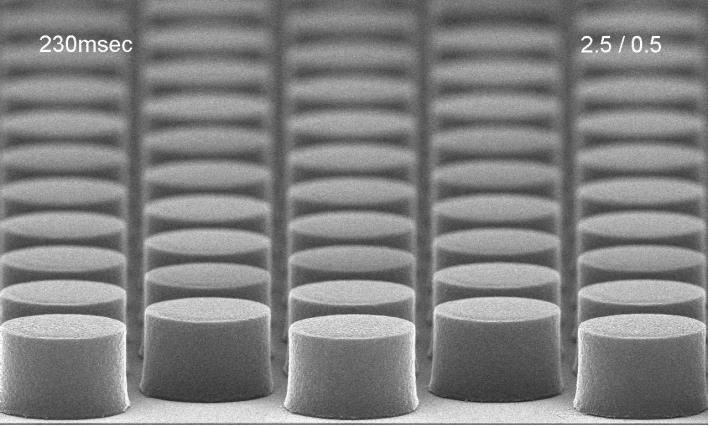
Ⅰ、EPI 612 series
Resist Film Thickness:1.5~4.5um
Property:
1. High resolution;
2. Excellent etching resistance;
3. High thermal resistance;
4. Wide process margin.
Ⅱ、Application Fields:
1. LED Lighting:
Applicable to traditional blue and green LEDs, high-brightness lighting, deep-ultraviolet LEDs and other lighting scenarios. As a core technology for sapphire substrate patterning, PSS technology can effectively improve the light extraction efficiency and service life of LED devices.
2. Display Applications:
Widely adopted in Mini/Micro LED, backlight display, and RGB direct display fields. With the accelerated industrialization of Mini/Micro LED, the market demand for high-performance PSS photoresist continues to grow steadily.
3. Automotive Electronics:
Applied to automotive lighting and vehicle display scenarios. Market demand keeps expanding alongside the rapid penetration of new energy vehicles and in-vehicle display technologies.
4. Gallium Nitride (GaN) Power Devices:
PSS technology can be applied to substrate patterning for next-generation high-efficiency GaN power devices, opening up new growth opportunities in the power semiconductor industry.
