
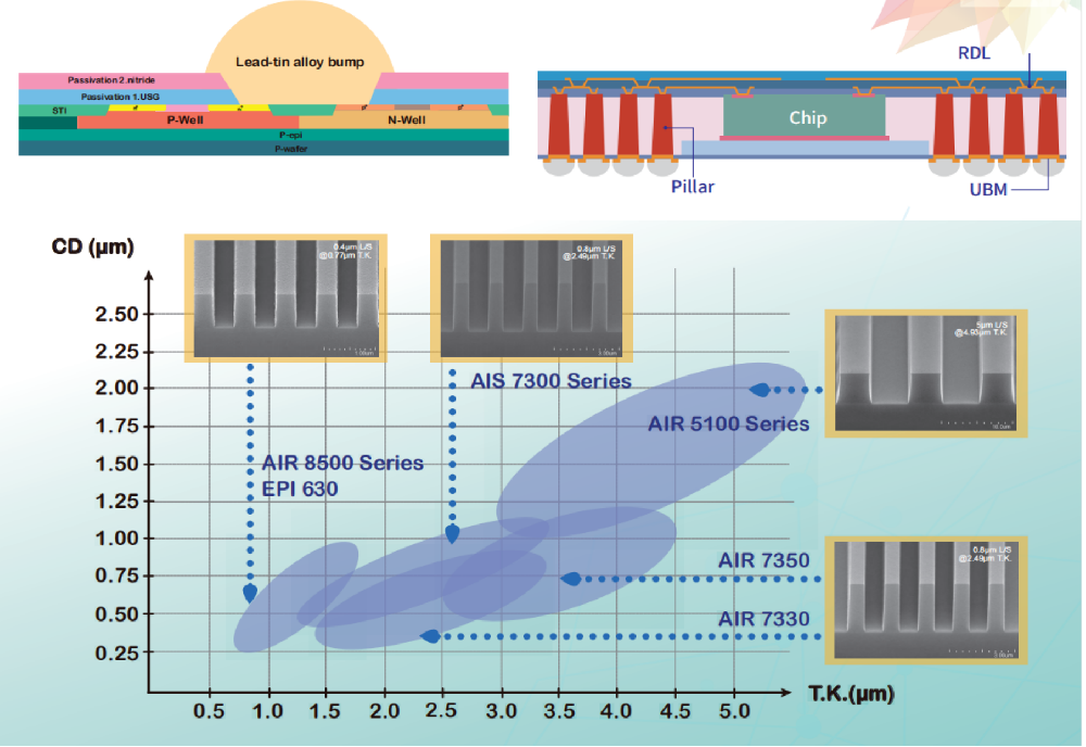
Ⅰ、AIR 8510
AIR 7330
AIR 5155
Resist Film Thickness:0.3~4um
Property:
1. High resolution;
2. Excellent etching resistance;
3. High thermal resistance;
4. High photo speed;
5. Wide process margin.
Application Fields:
1. Power Semiconductors and Discrete Devices:
I-line photoresist holds a market share of over 50% in the power semiconductor field. It is widely used as an etching mask and ion implantation protective layer for power devices such as MOSFETs, IGBTs, and diodes.
2. Micro-Electro-Mechanical Systems (MEMS) and Sensors:
It is applied to deep trench etching and patterning for the structures of MEMS accelerometers, gyroscopes, pressure sensors and other devices. It also covers microfabrication scenarios including TSV (Through-Silicon Via), microfluidic channels, and optical components. In addition, I-line grayscale lithography enables efficient fabrication of 2.5D/3D micro-nano structures such as microlens arrays.
3. Analog and Mixed-Signal Chips:
It is adopted in the 0.35 μm node process for analog ICs and radio frequency (RF) chips, which feature low requirements for line width but high emphasis on device matching and stability.
4. Advanced Packaging:
Thick-film I-line photoresist is extensively used in advanced packaging processes, including permanent protective layers for wafer-level packaging (WLP), redistribution layer (RDL) patterning, and bump fabrication.
5. Display Driver ICs (DDI) and Image Sensors:
It is applied to TFT array manufacturing, as well as thick-film lithography and passivation protection for LEDs and CMOS Image Sensors (CIS).
6. Mature IC Manufacturing Processes:
It is utilized for mass production of critical layers at the 0.35 μm to 0.30 μm process node for mid-to-low-end logic chips (MCUs), power management ICs (PMICs), automotive electronics and other products.
