Co., Ltd")


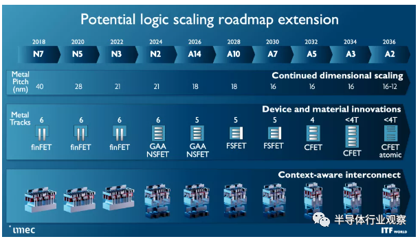
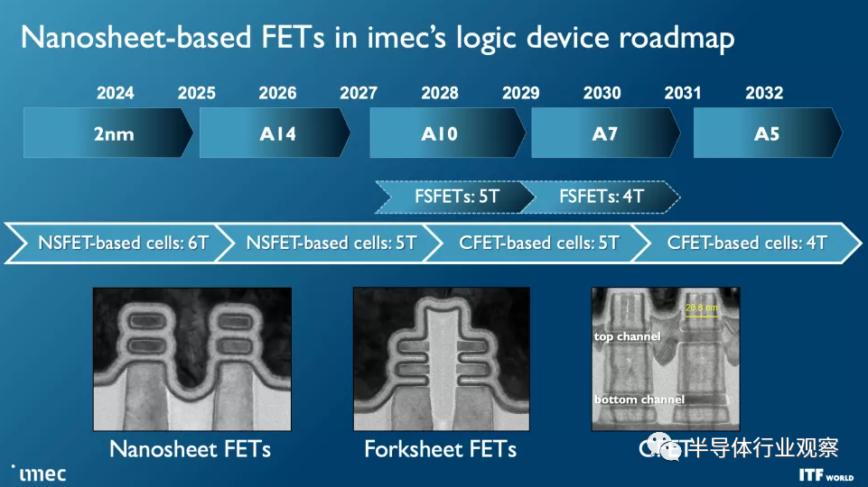
As a reminder, 10 angstroms equals 1 nanometer, so Imec's roadmap includes sub-"1 nanometer" process nodes. The roadmap outlines that standard FinFET transistors will last to 3nm and then transition to a new all-gate (GAA) nanosheet design that will enter high-volume production in 2024. Imec mapped the 2nm and A7 (0.7nm) Forksheet designs, followed by breakthrough designs such as CFET and atomic channel for A5 and A2 respectively.
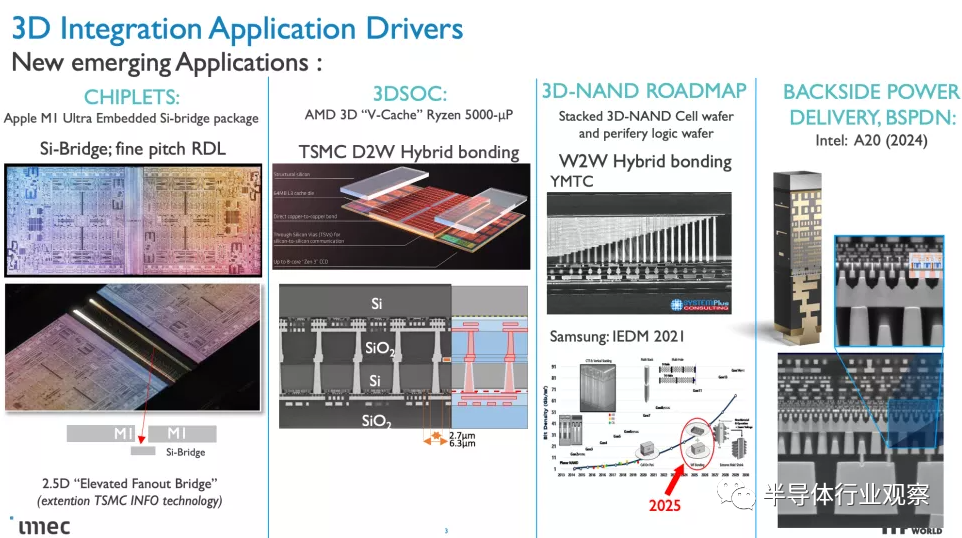
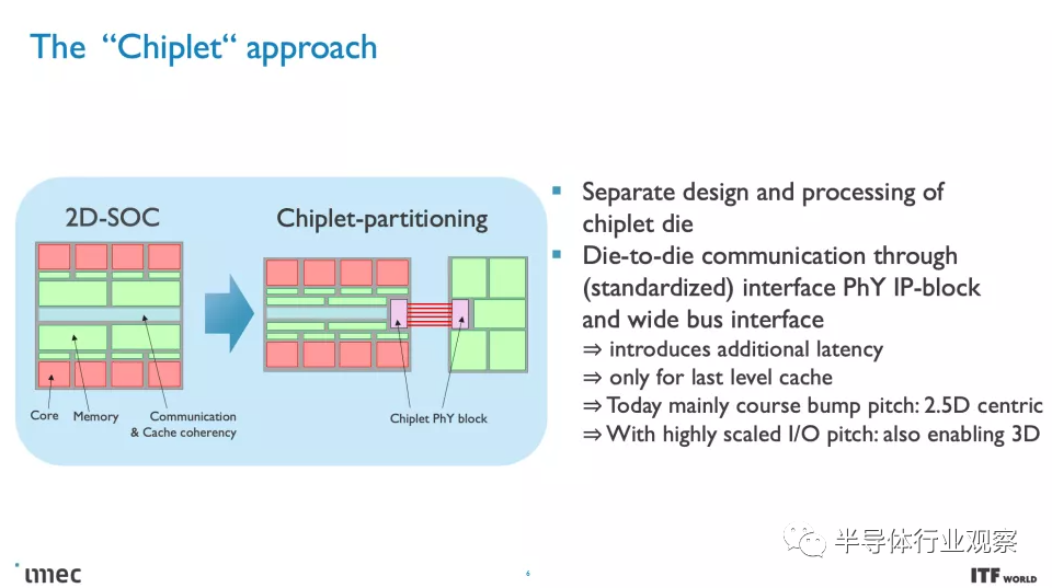
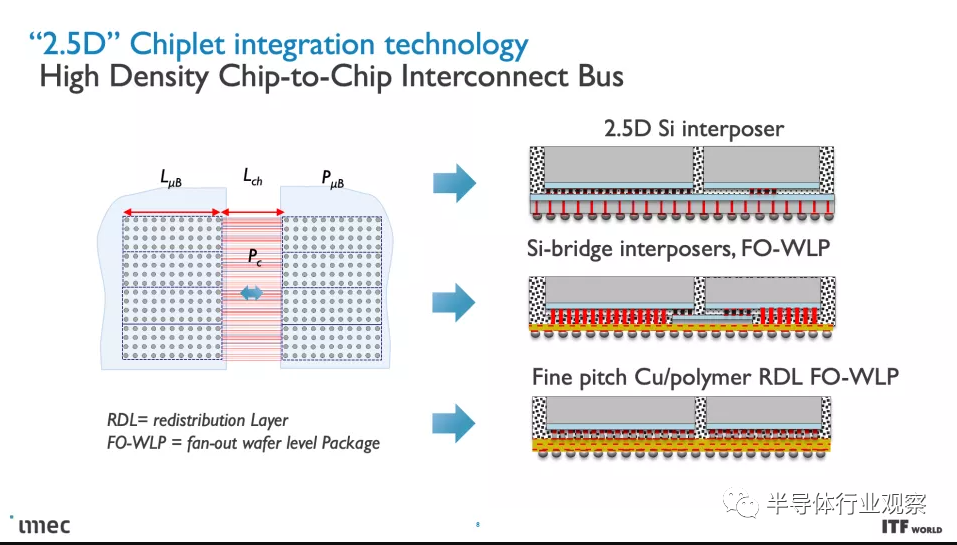
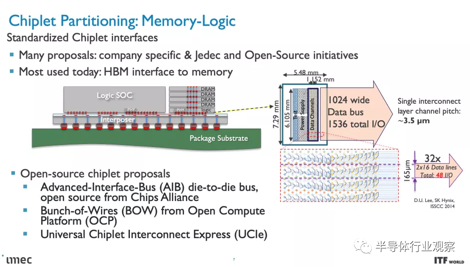
Over time, moving to these smaller nodes has become increasingly expensive, and the standard approach of building monolithic chips using single large chips has given way to smaller chips. Chiplet based designs break down the various chip functions into different chips connected together, enabling the chip to function as a cohesive unit-albeit with tradeoffs.
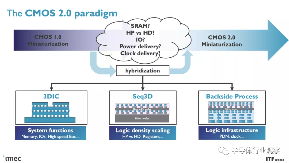
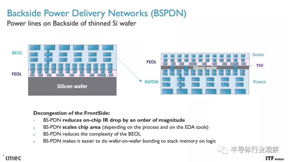
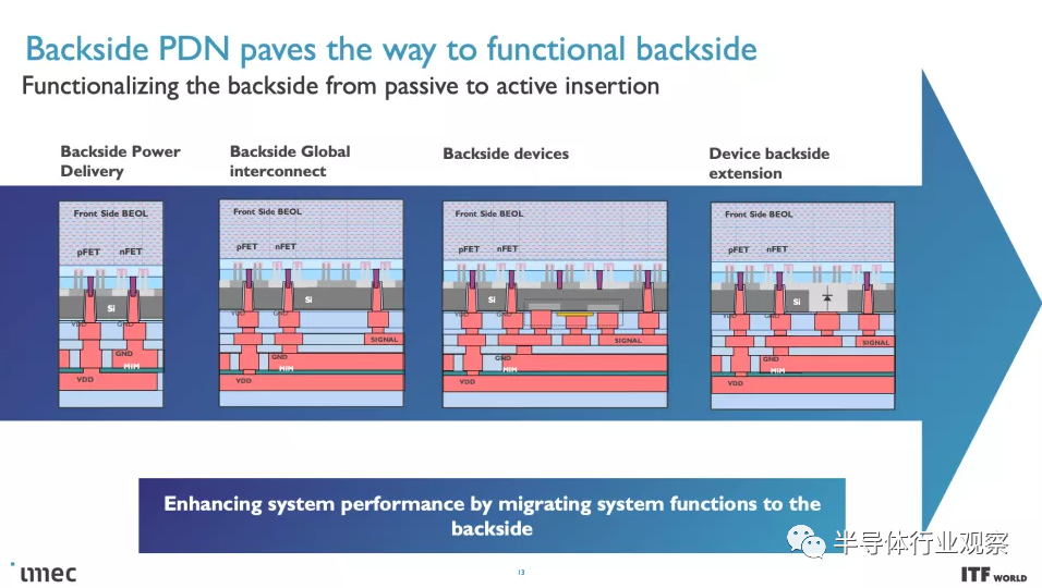
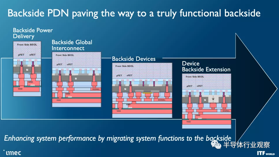
Imec's vision for the CMOS 2.0 paradigm involves breaking the chip down into smaller pieces, dividing the cache and memory into its own cells with different transistors, and then stacking them on top of other chip functions in a 3D arrangement. This approach would also rely heavily on the backside power supply network (BPDN), which routes all power through the backside of the transistor.
Let's take a closer look at the imec roadmap and the new CMOS 2.0 approach.
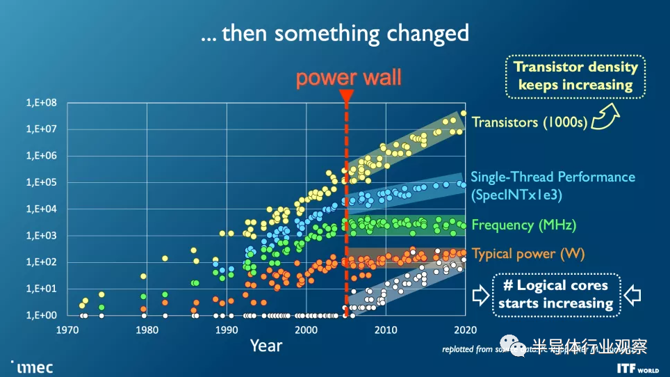
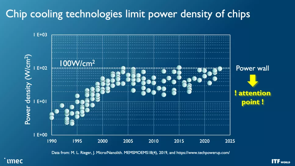
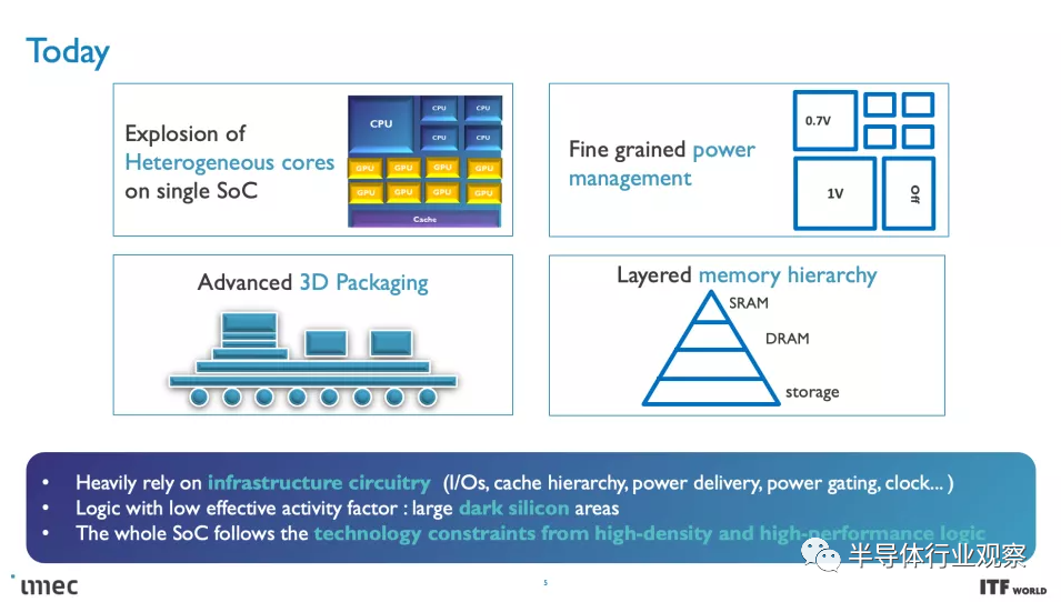
As you can see in the photo album above, the industry faces seemingly insurmountable challenges as nodes advance, but the demand for more compute power, especially machine learning and artificial intelligence, grows exponentially. This demand is not easy to satisfy. Costs skyrocket while power consumption for high-end chips steadily increases-power scaling remains a challenge as CMOS operating voltages stubbornly refuse to go below 0.7 volts, and the continued need to scale to larger chips presents power and cooling challenges that will require entirely new circumvention solutions.
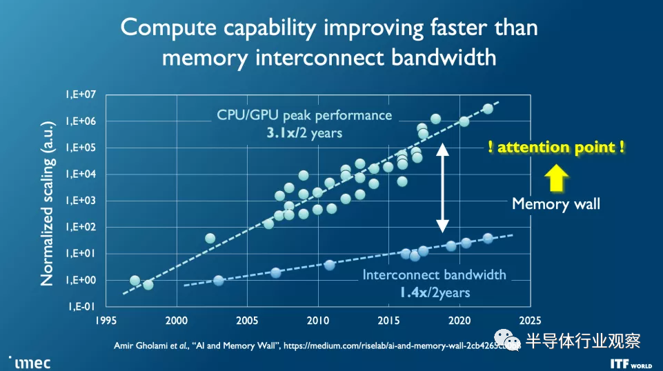
While transistor counts continue to double on the predictable Moore's Law path, other fundamental issues are increasingly becoming a problem with each new generation of chips, such as interconnect bandwidth limitations that lag significantly behind the computing power of modern CPUs and GPUs, hampering performance and limiting the effectiveness of these extra transistors.
imec transistor and process node roadmap
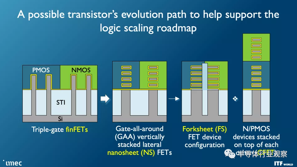
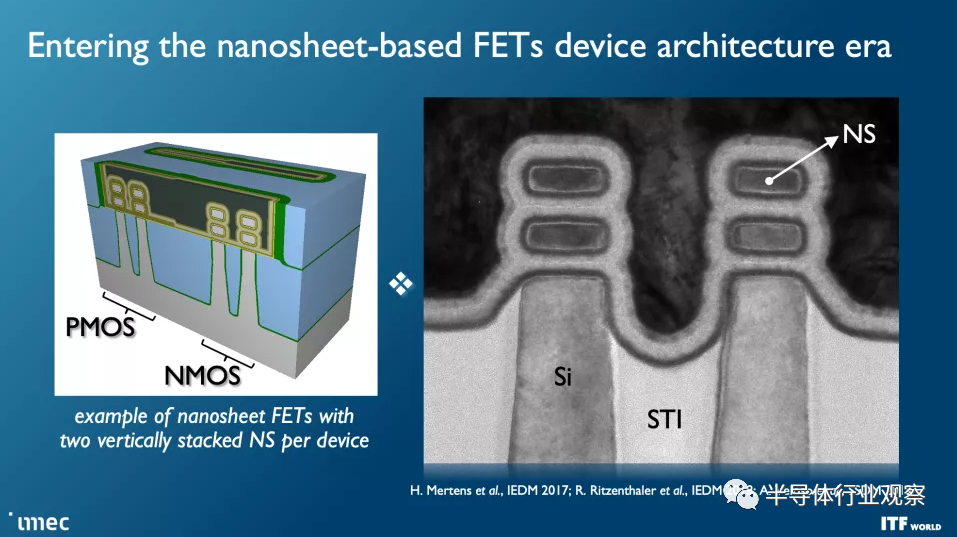
Faster, denser transistors are a priority, however, and the first wave of these transistors will be accompanied by Gate All Around (GAA)/Nanosheet devices debuting at the 2nm node in 2024, replacing the tri-gate FinFETs that power today's leading technologies. GAA transistors give transistor density and performance improvements, such as faster transistor switching, while using the same drive current as multiple fins. Leakage is also significantly reduced because the channel is completely surrounded by the gate, and adjusting the thickness of the channel can optimize power consumption or performance.
We have seen several chip manufacturers adopt different variants of this transistor technology. Industry leader TSMC plans to mass-produce its N2 node with GAA by 2025, so it will be the last to adopt the new transistor. Intel's four-layer RibbonFET with "Intel 20A" process nodes features four stacked nanosheets, each completely surrounded by a gate, and will debut in 2024. Samsung is the first to produce GAA for shipping products, but nodes with small batches of SF3E pipe-cleane won't see mass production. Instead, the company will launch its advanced nodes for high-volume manufacturing in 2024.
Just to remind you, 10 angstroms (A) equals 1 nanometer. This means that A14 is 1.4 nanometers and A10 is 1 nanometer, and we will enter the sub-1 nanometer era with A7 in the 2030 time frame. Keep in mind, however, that these metrics often don't match the actual physical size on the chip.
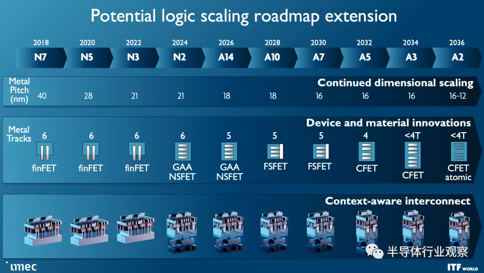
Imec expects forksheet transistors to start at 1nm (A10) all the way to the A7 node (0.7 nm). As you can see in the second slide, this design stacks NMOS and PMOS separately, but uses a dielectric barrier to separate them for higher performance and/or better density.
Complementary FET (CFET) transistors will further shrink footprint when they first appear as 1nm nodes (A10) in 2028, allowing for a denser library of standard cells. Eventually, we'll see versions of CFET with atomic channels, further improving performance and scalability. CFET transistors (you can read more about them here) stack N-type and PMOS devices together for higher density. CFET should mark the end of nanosheet device scaling and the end of the visible roadmap.
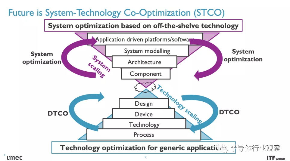
However, other important technologies will be needed to break down performance, power and density scaling barriers, which imec envisions will require new CMOS 2.0 paradigms and system technology collaborative optimization (SCTO).
STCO and back power
At the highest level, system technology co-optimization (STCO) requires rethinking the design process by modeling the requirements of the system and target applications, and then using this knowledge to inform design decisions to create chips. This design approach typically results in "breaking down" functional units that are typically part of a monolithic processor, such as power supply, I/O, and cache, and breaking them down into separate units to target the required performance characteristics by using different methods to optimize the transistors of each unit type, which then also increases costs.
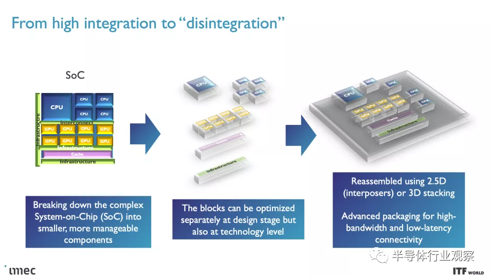
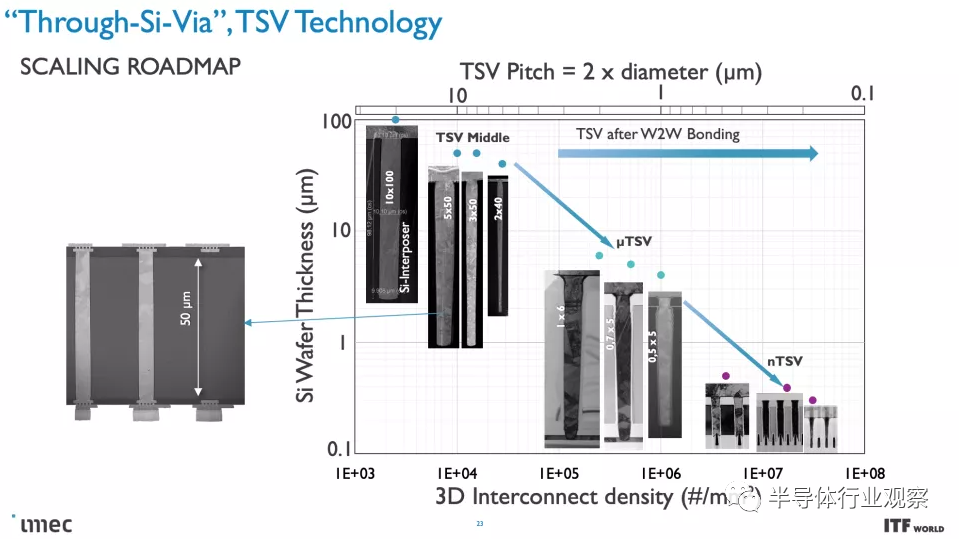
One of the goals of fully decomposing standard chip designs is to split cache/memory into their own different layers in a 3D stack design (see more below), but this requires reducing complexity at the top of the chip stack. Retrofitting the Back End of Line (BEOL) process, with an emphasis on connecting transistors together and enabling communication (signals) and power transmission, is key to this effort.
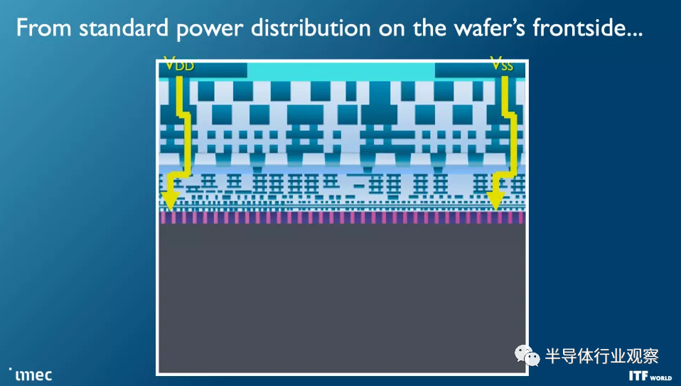
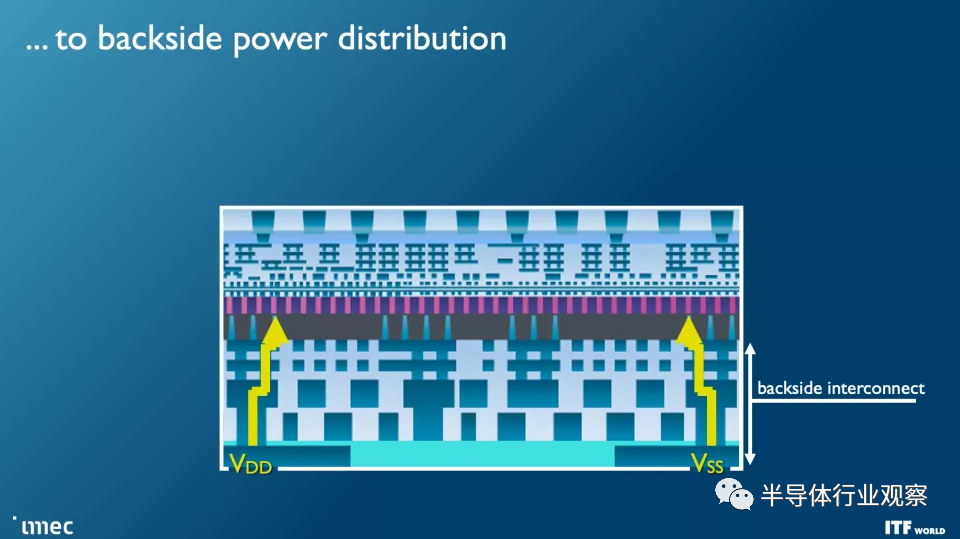
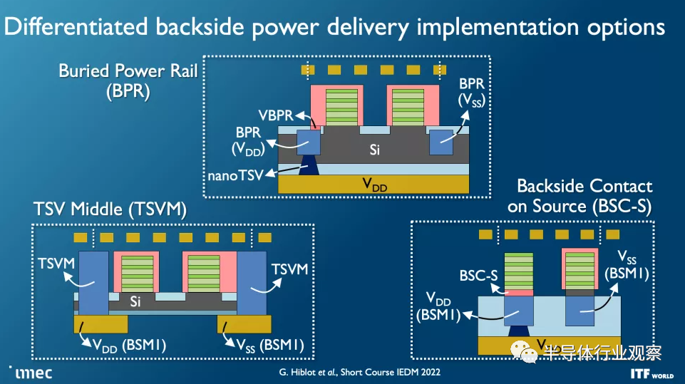
Unlike today's designs, which transfer power from the top of the chip down to the transistors, backside power distribution networks (BPDN) use TSVs to route all power directly to the backside of the transistors, separating power transfer from the data transfer interconnects that remain inside them at the normal location on the other side. Separating the power circuitry and data transfer interconnects improves voltage drop characteristics, enabling faster transistor switching while enabling denser signal routing at the top of the chip. Signal integrity is also beneficial because simplified wiring allows for faster connection of resistors and capacitors.
Moving the power supply network to the bottom of the chip makes wafer-to-wafer bonding easier on top of the die, freeing up the potential for stacking logic on top of memory. Imec even envisions the possibility of transferring other functions to the backside of the wafer, such as global interconnects or clock signals.
Intel has announced its own version of BPDN technology, called PowerVIA, which will debut in 2024 as Intel 20A node. Intel will reveal more details about the technology at an upcoming VLSI event. At the same time, TSMC also announced that it will introduce BPDN into its N2P nodes in 2026, so this technology will lag behind Intel for a long time. There are also rumors that Samsung will adopt the technology at its 2nm node.
CMOS 2.0: The Road to True 3D Chips
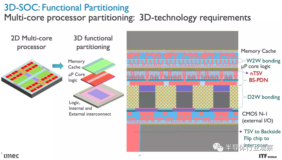
CMOS 2.0 is the culmination of imec's vision for future chip design, covering all 3D chip designs. We've seen AMD's memory stack for Gen 2 3D V-Cache, stacking L3 memory on top of the processor to boost memory capacity, but imec envisions the entire cache hierarchy contained in its own layers, with L1, L2, and L3 caches stacked vertically on its own chip above the transistors that make up the processing core. Each level of cache will be created using the transistor best suited for that task, meaning the old node of SRAM, as SRAM scaling speeds begin to slow down dramatically,
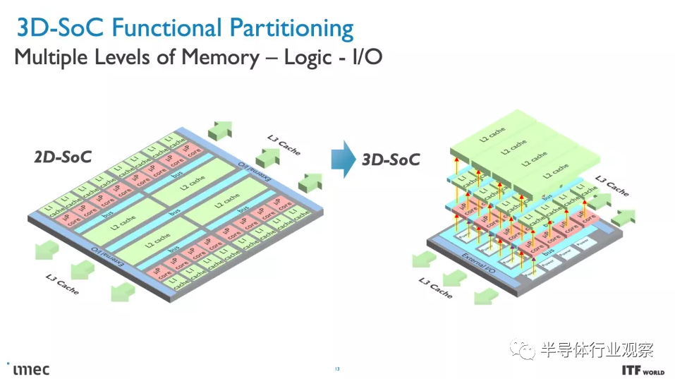
This is becoming increasingly important. The shrinking size of SRAM results in cache occupying a higher percentage of die, resulting in increased cost per MB and discouraging chip manufacturers from using larger caches. Therefore, the cost reduction associated with moving the cache of the 3D stack to a less dense node may also result in a larger cache than we have seen in the past. If implemented properly, 3D stacking can also help mitigate latency issues associated with larger caches.
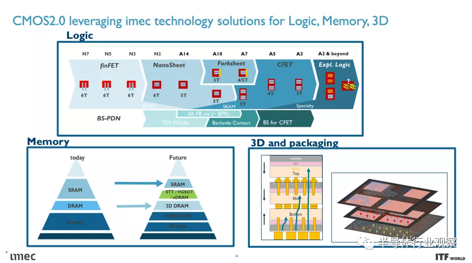
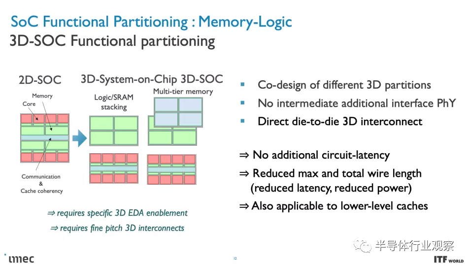
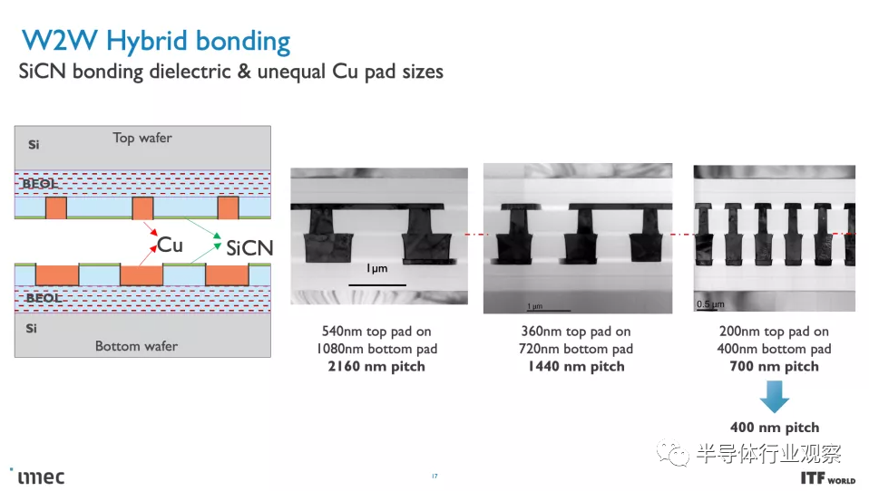
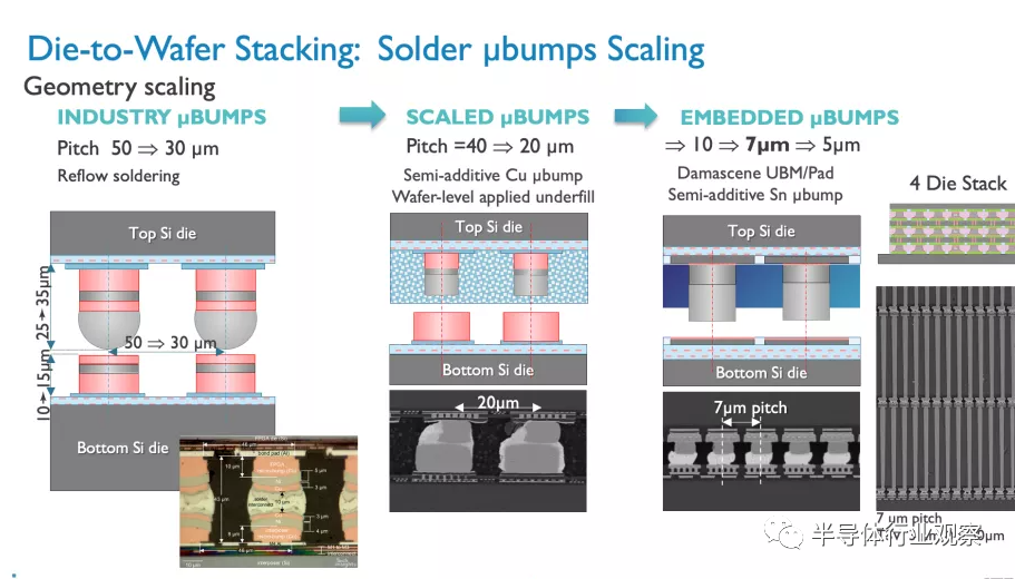
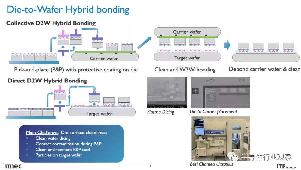
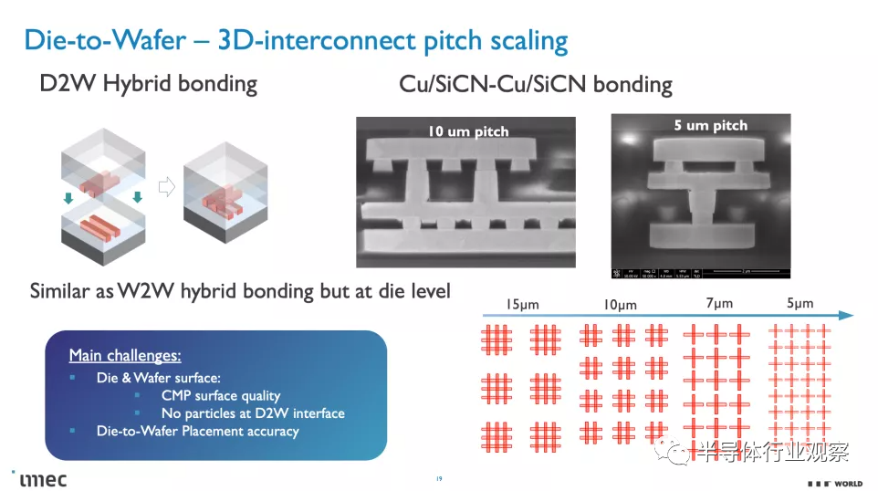
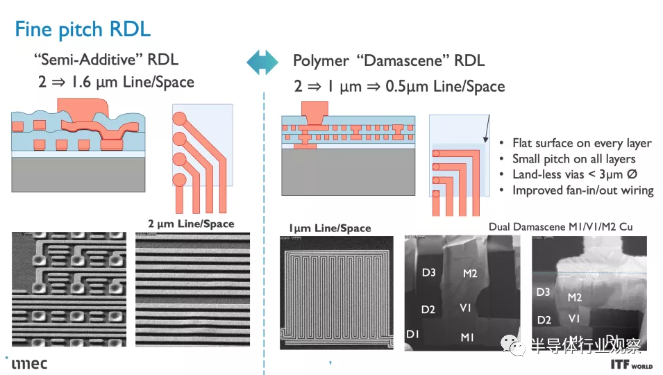
These CMOS 2.0 technologies will utilize 3D stacking techniques such as wafer-to-wafer hybrid bonding to form direct chip-to-chip 3D interconnects.
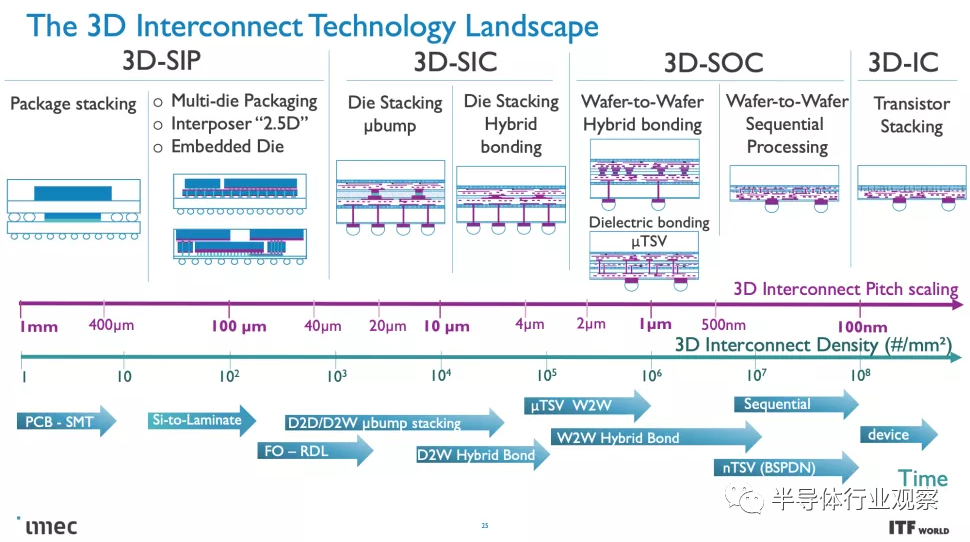
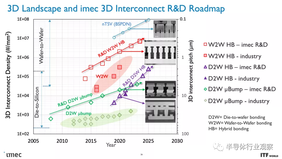
As you can see in the album above, Imec also has a 3D-SOC roadmap outlining the continued scaling of interconnects that bind 3D designs together to enable faster, denser interconnects in the future. These advances will be realized over the next few years by using newer types of interconnects and processing methods.